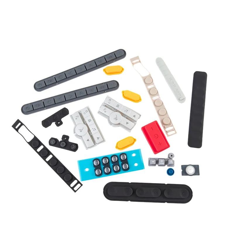
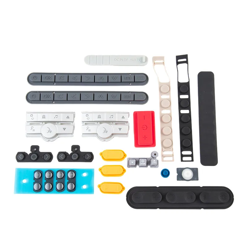
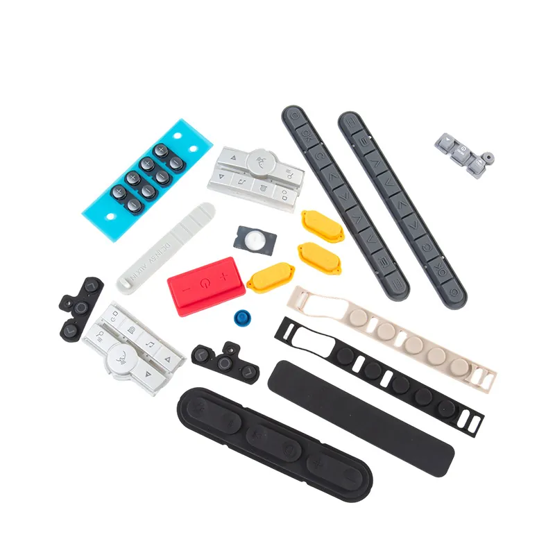
What Is a Conductive Silicone Keypad?
A conductive keypad carries the signal, so its performance is measured electrically as well as mechanically. Two parameters decide whether it works in the field: contact resistance and its stability over actuation life. Contact resistance drifts when the conductive element oxidises, when the pill geometry deforms permanently, or when contamination reaches the contact pad. We mould conductive silicone keypads using carbon pills or conductive ink tracks, and we treat the electrical target as a manufacturing specification rather than a by-product of the moulding.
Applications
- Industrial controllers and panel instruments with PCB-contact switching
- Handheld and outdoor devices requiring sealed interfaces
- Machine pendants, remote controls and operator terminals
- Laboratory and test instruments
- Consumer and commercial electronics interfaces
The Engineering Problem
The failure mode we see most is contact resistance drift: the device works when new and becomes unreliable after months of use, with keys needing a harder press to register. The root cause is usually a combination of conductive element wear, contamination at the contact pad, and web geometry that lets the pill deform instead of making clean contact. It is fixable, but only by engineering the conductive element and the web together.
Product Features
- Carbon pill or conductive-ink construction selected against your switching target
- Contact resistance specified and measured, not assumed
- Pill geometry designed to make clean contact without permanent deformation
- Web geometry tuned so actuation force produces reliable switching
- Sealed perimeter option for wet and washdown environments
- Legend and graphic options consistent with non-conductive products
- Actuation-life testing before approval where required
Material Options
| Material | When we would choose it |
|---|---|
| Silicone with carbon pills | The standard approach for direct PCB contact switching |
| Silicone with conductive ink | Where a lower profile or different contact geometry is needed |
| Translucent silicone | Where backlighting is required alongside conduction |
| LSR grades | High-precision and long-life variants where the switching target is demanding |
Material Properties
| Property | Typical value / comment |
|---|---|
| Contact resistance | Specified per project. Drift over life matters more than the initial value |
| Hardness | Typically 40-60 Shore A. Affects both feel and the contact force available |
| Tear resistance | Determines how the web and pill survive repeated cycling |
| Compression set | Stability of the pill under sustained or repeated load |
| Chemical resistance | Selected against the cleaning agents and contamination the device sees |
Specifications
| Parameter | What we work to |
|---|---|
| Dimensions | Moulded to drawing; key positions matched to your PCB pad layout |
| Tolerance | ±0.05 mm on critical moulded dimensions |
| Operating temperature | Silicone -60 to +230 C (compound dependent) |
| Hardness | 20-80 Shore A; conductive keypads typically 40-60 Shore A |
| Colour | Body colours to sample; conductive elements are typically dark |
| Surface finish | Smooth, matte or textured; legends printed or laser-etched |
| Waterproof / sealing | Integrated perimeter seal designed together with the housing gland |
| Chemical resistance | Compound matched to your cleaning and contamination exposure |
Production Process
- PCB pad layout, switching target and actuation life collected
- Conductive element and web geometry designed together
- Compound, hardness and pill specification proposed
- Mould built with legends where required
- First-article samples tested for contact resistance, actuation force and sealing
- Production with in-process checks on the conductive element
- Electrical and dimensional records issued with shipment
Customization
- Carbon pill or conductive ink, selected against your switching target
- Pill geometry and contact area sized to your PCB pads
- Multiple conductive zones where a key performs more than one function
- Integrated perimeter seal and connector boots
- Backlighting combined with conduction
- Legend and graphic treatment matching the rest of your interface
Tooling & Prototyping
Conductive keypad tooling must control both the mechanical geometry and the placement of the conductive element, so the mould design is more demanding than for a standard keypad. First-article samples are tested electrically before approval. Tooling cost is refundable against volume production.
MOQ, Quality Control & Packaging
| Item | How it is handled |
|---|---|
| MOQ | Quoted per project against tooling, part size and the conductive specification. |
| Quality control | Material verification, in-process checks, dimensional inspection, contact resistance measurement and actuation checks |
| Packaging | Trayed to protect conductive elements and printed surfaces |
| Documentation | Electrical and dimensional records; artwork approval record |
Material Compliance
The silicone compound we mould carries third-party SGS reports covering EU RoHS 2015/863, REACH SVHC, phthalates, PAHs, halogen, US FDA 21 CFR 177.2600, LFGB Section 30 and 31, and GB 4806.16-2025 - all Pass. A part's compliance depends on the compound grade, the colour and the process, so the grade is matched to your requirement at quotation stage. See the material compliance page for the report numbers.
Conductive Silicone Keypads — Frequently Asked Questions
It depends on the conductive element, the contact pad finish and the actuation force. Send your switching target and your PCB pad specification and we will confirm what is achievable rather than quoting an optimistic number.
Almost always contact resistance drift: the conductive element wears, or the web geometry allows the pill to deform permanently rather than making clean contact. Both are design issues and both are solvable.
Carbon pills suit conventional PCB contact switching and are robust. Conductive ink suits lower profiles and different contact geometries. The choice depends on your pad layout, force target and life expectancy, and we will recommend one.
Yes. The perimeter seal is designed into the same moulded part, and the conductive element is protected inside the sealed volume.
Where the programme requires it, samples are tested for contact resistance stability over actuation before approval. Tell us the life target at RFQ stage.
Yes, and it is usually the better design. Integrating the perimeter seal into the keypad removes an assembly step and a potential leak path.
Related Products
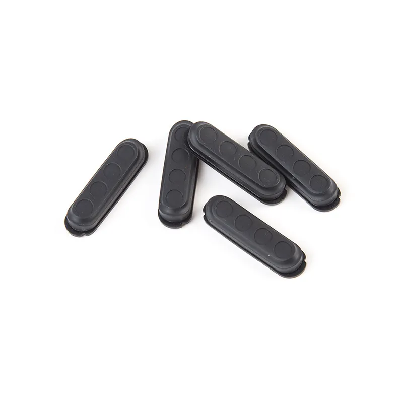
Silicone Keypads
Non-conductive keypads with tactile feedback, graphics and backlighting.
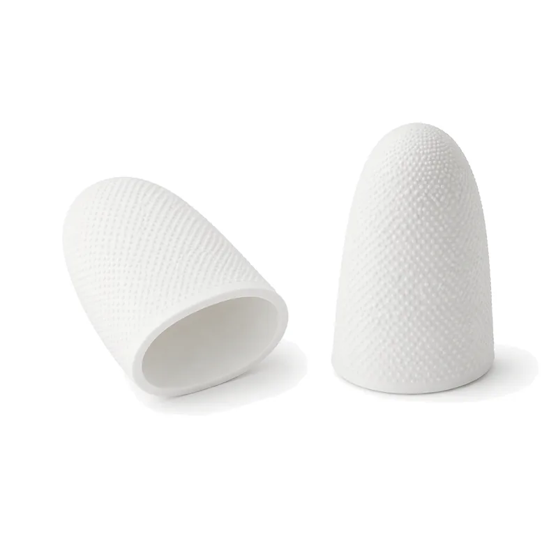
Protective Sleeves & Covers
Sealed silicone boots and sleeves for connectors and joints.
Silicone Molding
Compression and LSR moulding for precision silicone interfaces.
Related Industries
Robotics
Sealing, damping and protective components for industrial, collaborative and service robots.
Industrial Automation
Seals, gaskets and moulded parts for actuators, conveyors and machine frames.
Electronics
Enclosure sealing, insulation and interface components for controllers and instruments.
Drones & UAV
Waterproof sealing and vibration isolation for airframes and payloads.
Related Case Study
Silicone Components for a Humanoid Robot Finger
Contact and sealing parts on an articulated finger, built for wear and consistent tactile behaviour.
Gripper Protective Sleeves for Robot Fingers
Sleeves that sit over the robot fingers, supplied for laundry handling and parcel sorting.